 |
| |
Atmel ATtiny AVR - TPI Interface - Device Library - Overview |
|
|
|
|
|
| |
The 'ATtiny TPI' Device Library supports In-System Programming (ISP) of the Atmel ATtiny AVR microcontroller family via the 2-wire TPI (Tiny Programming Interface). This solution is aimed at high throughput production users who require the fastest possible programming of the on-chip FLASH memory of any ATtiny TPI AVR microcontroller.
Supported devices include ATtiny10, 9, 4, 5 and 20. The 'Low-voltage' and 'High Voltage +12V Vpp' algorithms are both supported. |
| |
|
|
|
 |
Main Features |
|
- High-speed In-System Programming (ISP) support of Atmel ATtiny AVR microcontrollers via the 2-wire TPI (Tiny Programming Interface)
- Supports programming the on-chip FLASH, Fuse and Lock Bits of ATtiny TPI AVR microcontrollers
- Uses the proprietary Atmel 2-wire TPI (Tiny Programming Interface) to program the target device
- Supports low-voltage (+5V) TPI programming mode
- Supports high-voltage (+12V Vpp on RESET pin) TPI programming mode
- Very high-speed programming due to local data storage and optimised programming algorithms
- Optimised line driver circuit for TPI DATA line to allow bi-directional communications
- Programmers can be used in "Standalone Mode" (no PC) - Up to 64 x ATtiny 'Programming Projects' can be stored inside an ISPnano programmer
- Supports high-speed program / verify of the ATtiny on-chip FLASH in a singe operation.
- Optimised Erase operation supports independent erasing of FLASH and Configuration Section
- Supports programming of non volatle Fuse Bits
- Supports programming of the "Security Fuses" (Lock Bits) to protect code from being read out
- Supports reading of on-chip RC Oscillator Calibration Byte
|
 |
Programmers supporting ATtiny TPI |
|
|
This 'Device Library' is compatible with any of the Equinox programmers listed below:

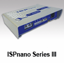   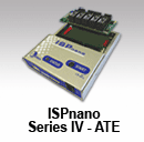
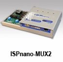 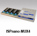 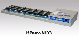
Important notes:
- The ISPnano Series 3, Series S3 ATE, Series 4 ATE and GANG programmers require a 'Device Library' per programmer channel.
- The ISPnano-MUX programming systems only require one licnese per programmer.
|
 |
Low-voltage ATtiny TPI Programming Interface |
|
|
The 'Low-voltage ATtiny TPI' interface uses 3 pins for programming the Target Device as detailed in the table below.
|
PDI Signal
Name |
Signal description |
Direction from programmer |
Pin name on ATtiny device |
|
TPI_CLK
|
TPI Clock Signal |
Output |
TPI_CLK |
|
TPI_DATA |
PDI Data Signal
(bi-directional) |
Bi-directional |
TPI_DATA |
|
/RESET |
RESET pin |
Output |
RESET |
The ATtiny device must be powered at +5.0V during the programming process. It is not possible to program the device at any voltage lower than +5.0V.
|
 |
High-voltage (+12V Vpp) ATtiny TPI Programming Interface |
|
|
The 'High-voltage ATtiny TPI' interface uses 3 pins for programming the Target Device as detailed in the table below.
|
PDI Signal
Name |
Signal description |
Direction from programmer |
Pin name on ATtiny device |
|
TPI_CLK
|
TPI Clock Signal |
Output |
TPI_CLK |
|
TPI_DATA |
PDI Data Signal
(bi-directional) |
Bi-directional |
TPI_DATA |
|
/RESET +12Vpp |
RESET pin |
Output |
RESET |
The ATtiny device must be powered at +5.0V during the programming process. The programmer must apply a +12V Vpp voltage to the RESET pin in order to enter this mode. This mode is usually only used if the RSTDIBL (RESET pin disable) fuse has been set.
|
| |
| |
Device Support (by family) |
|
|
|
|
|
| This product supports devices from the families listed below: |
| |
Atmel (Microchip):
-
ATtiny (High voltage TPI Interface) : ATtiny TPI algorithm requiring that +12V Vpp is applied to the RESET pin.
-
ATtiny (Low voltage TPI Interface)
|
| |
|
Please note:
Not all devices may be supported within a family.
Please see the Detailed Device Support List for a list of all devices which the product supports.
|
| |
|  |


|